ÉPI (Puce à bord) la technologie est un processus de fabrication où Red, Vert, et bleu (RVB) les puces à diodes électroluminescentes sont encapsulé directement sur le circuit imprimé (PCB).
Contrairement aux méthodes d'emballage traditionnelles, La technologie COB élimine le besoin de supports de perles de lampe indépendants (ou les jambes), intégrer les puces nues directement sur le substrat. Ce processus permet non seulement une densité de copeaux plus élevée, mais crée également un, surface émettrice de lumière uniforme. Parce que les puces RVB sont si étroitement intégrées les unes aux autres, Les écrans COB peuvent atteindre une gamme de couleurs plus large, reproduisant ainsi des images plus réalistes.
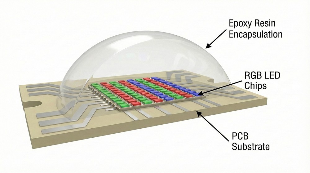
En termes simples, dans la même zone d'affichage, La technologie COB peut accueillir beaucoup plus de puces LED que les technologies traditionnelles (comme SMD ou DIP), résultant en une amélioration massive de la résolution d’affichage.
Differences Between COB and SMD Packaging Technologies
Before COB technology became popular, LED displays mainly relied on CMS (Surface Mounted Diode) et DIP (Dual in-line Package) technologies. Among them, SMD long occupied the mainstream position due to its relatively high density.
1. Structure and Connection Method
- Technologie CMS: LED components are mounted on the PCB surface via wire bonding and fixed using a soldering machine. While this method is mature, improper control of the soldering process (such as weak or excessive soldering) can lead to connection failures. En plus, SMD components protrude from the circuit board surface, making them vulnerable to physical impact or environmental factors like moisture.
- Technologie COB: Chips are bonded directly to the circuit board using adhesives, eliminating the need for metal wires. This connection method is more stable and greatly reduces the risk of failure caused by soldering issues.
2. Pixel Pitch and Size
- Technologie CMS: Usually limited by component size (generally larger than 0.5 mm), making it difficult to achieve extremely small pitches.
- Technologie COB: Can handle micron-level chips without needing space for wires. This allows for a tighter Pixel Pitch, which is crucial for manufacturing high-resolution (par ex., 4K, 8K) Micro LED displays.
Four Core Advantages of COB LED Technology
Now that we understand the basic principles of COB, let’s look at the revolutionary improvements it brings to practical applications:
1. Extreme Pixel Pitch and Resolution
Pixel pitch determines the fineness of a display. Because COB technology eliminates brackets and pins, pixel points can be packed very tightly. A smaller pixel pitch means higher pixel density, enabling COB displays to easily achieve 4K or even higher resolutions.
For the viewer, this means that even when watching the screen from a close distance, there is almost no visible “pixellisation” (screen door effect), resulting in a much smoother and more detailed visual experience.
2. Superior Reliability and Protection
Traditional SMD screens are prone to “dead pixels” caused by bumps and are sensitive to environmental moisture. COB technology achieves a leap in reliability:
- Collision Resistance: The surface of a COB screen is typically covered with a layer of epoxy resin. The surface is flat and smooth, offering extremely strong protection against impact.
- Dust and Water Resistance: Thanks to the overall encapsulation process, the protection rating of COB displays can typically reach IP54 (compared to SMD, which is usually only IP20 or IP30), effectively resisting dust and moisture intrusion.
- Meilleure dissipation thermique: Direct encapsulation on the PCB reduces thermal resistance, resulting in better heat dissipation and extending the lifespan of the screen.
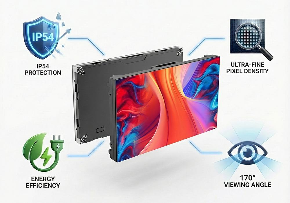
3. Higher Energy Efficiency
For large display equipment that needs to run 24/7, energy consumption is a huge cost factor. COB LED technology offers higher luminous efficiency and lower heat loss compared to SMD technology. Over long-term use, COB displays can significantly reduce operating costs, making them more energy-saving and environmentally friendly.
4. Upgraded Visual Experience
COB technology is not just “durable”; its image quality performance is also superior:
- Ultra-Wide Viewing Angle: Utilizing Flip Chip technologie, COB screens can achieve a viewing angle of up to 170 degrés, maintaining consistent color accuracy regardless of the angle from which it is viewed.
- High Contrast: La technologie COB permet d'obtenir des noirs plus profonds et une luminosité plus élevée, augmentant considérablement les taux de contraste. Cela le rend idéal pour les lieux ayant des exigences de qualité d'image extrêmement élevées., tels que les studios de conception architecturale, salles de conférence haut de gamme, studios de diffusion, et installations de recherche médicale.
Pensées finales
La technologie LED COB représente la dernière avancée en matière de processus d'emballage LED. Par raccourcir le pas des pixels, amélioration des indices de protection, réduire la consommation d'énergie, et optimisation des effets visuels, il redéfinit les normes des écrans haut de gamme. Que ce soit pour des affichages commerciaux, centres de commandement, ou home cinéma haut de gamme, La technologie COB a démontré son immense potentiel en tant que “l'avenir de la technologie d'affichage.”